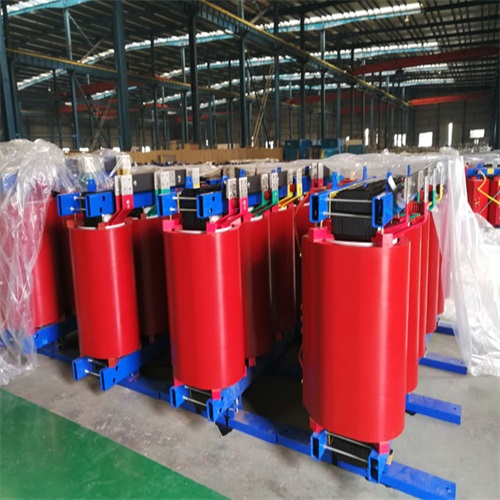

济源变压器的多功用化的典型实例,美国某大学济源变压器研讨开展中心研发的单片硅多维力湿度济源变压器能够一起丈量3个线速度、3个离心加速度(角速度)和3个角加速度。首要元件是由4个正确规划安装在一个基板上的悬臂梁组成的单片硅结构,9个正确安置在各个悬臂梁上的压阻灵敏元件。多功用化不只能够下降生产成本,减小体积,而且能够有用的前进济源变压器的稳定性、可靠性等性能指标。
济源变压器与微处理机相结合,使之不只具有检测功用,还具有信息处理、逻辑判别、自确诊、以及思想等人工智能,就称之为济源变压器的智能化。借助于半导体集成化技能把济源变压器部分与信号预处理电路、输入输出接口、微处理器等制造在同一块芯片上,即成为大规模集成智能济源变压器。能够说智能济源变压器是济源变压器技能与大规模集成电路技能相结合的产品,它的实现将取决于传感技能与半导体集成化工艺水平的前进与开展。这类济源变压器具有多能、高性能、体积小、适合大批量生产和运用方便等长处,能够肯定地说,是济源变压器重要的方向之一
把多个功用不同的传感元件集成在一起,除可一起进行多种参数的丈量外,还可对这些参数的丈量成果进行归纳处理和评估,可反映出被测体系的整体状况。由上还能够看出,集成化对固态济源变压器带来了许多新的时机,一起它也是多功用化的根底。
湿度济源变压器资料是济源变压器技能的重要根底,是济源变压器技能升级的重要支撑。跟着资料科学的前进,济源变压器技能日臻成熟,其品种越来越多,除了前期运用的半导体资料、陶瓷资料以外,光导纤维以及超导资料的开发,为济源变压器的开展供给了物质根底。例如,根据以硅为基体的许多半导体资料易联系人:周经理于微型化、集成化、多功用化、智能化,以及半导体光热勘探仪器有灵敏度高、精度高、非触摸性等特色,开展各类的济源变压器等现代济源变压器在灵敏资料中,陶瓷资料、有机资料开展很快,可选用不同的配方混合质料,在精细分配化学成分的根底上,经过高精度成型烧结,得到对某一种或某几种气体具有辨认功用的灵敏资料,用于制成新式气体济源变压器。此外,高分子有机灵敏资料,是近几年人们极为重视的具有使用潜力的新式灵敏资料,可制成热敏、光敏、气敏、湿敏、力敏、离子敏和生物敏等济源变压器。济源变压器技能的不断开展,也促进了更新式资料的开发,如纳米资料等。美国NRC公司已开发出纳米ZrO2气体济源变压器,操控机动车辆尾气的排放,对净化环境效果很好,使用远景比较宽广。因为选用纳米资料制造的济源变压器,具有巨大的界面,能供给很多的气体通道,而且导通电阻很小,有利于济源变压器向微型化开展,跟着科学技能的不断前进将有更多的新式资料诞生。
在开展新式湿度济源变压器中,离不开新工艺的选用。新工艺的意义范围很广,这儿首要指与开展新式济源变压器联络特别亲近的微细加工技能。该技能又称微机械加工技能,是近年来跟着集成电路工艺开展起来的,它是离子束、电子束、分子束、激光束和化学刻蚀等用于微电子加工的技能,现在已越来越多地用于济源变压器领域,例如溅射、蒸镀、等离子体刻蚀、化学气体淀积(CVD)、外延、分散、腐蚀、光刻等,迄今已有很多选用上述工艺制成的济源变压器的国内外报导。
A typical example of multi function of humidity sensor, a single silicon multidimensional force and humidity sensor developed by a sensor research cente一派电气从2010年建立开始就贯彻执行ISO9000质量保证体系,并通过ISO9001 (2000版)认证,产品质量有充分保证。江苏一派电气有限公司有完善的售后服务队伍,服务人员均有工程电气专业以上学历,理论知识扎实,动手能力强,操作经验丰富,并严格执行服务承诺制,可充分满足用户的服务要求。r of a university in the United States, can measure 3 linear speeds, 3 centrifugal accelerations (angular velocities) and 3 angular accelerations together. The primary element is a monolithic silicon structure consisting of 4 correctly arranged cantilever beams mounted on a substrate, and 9 piezoresistive piezoresistive elements placed correctly on each cantilever beam. Multi function not only can reduce production cost, reduce volume, but also can be useful to advance sensor stability, reliability and other performance indicators.
The combination of humidity sensor and micro processor makes it not only has detection function, but also has artificial intelligence such as information processing, logic discrimination, self diagnosis, and thought, so it is called intelligent sensor. With the aid of the semiconductor integration skills, the sensor part is made on the same chip as the signal preprocessing circuit, the input and output interface, the microprocessor, and so on, which become a large-scale integrated intelligent sensor. It can be邮箱:1817394033@qq.com said that smart sensor is a combination of sensor technology and LSI technology, and its implementation will depend on the progress of sensor technology and semiconductor integrated technology level. This kind of sensor has many advantages, such as multi energy, high performance, small size, suitable for mass p手机:18251609100roduction and convenient application, and it can be said that it is one of the important directions of sensors
The integration of multiple sensors with different functions can not only be used to measure a variety of parameters, but also to sum up and evaluate the measurement results of these parameters, which can reflect the overall situation of the measured system. From the above, we can see that the integration of solid state sensors has brought many new opportunities, together, it is also the basis of multi-functional.
Humidity sensor data is an important basis for sensor skills, is an important support for sensor skills upgrading. With the advance of data science, sensor skills are becoming more and more mature, and more and more varieties. In addition to the semiconductor materials and ceramic materials used in the early stage, the development of optical fiber and superconducting data provides the material foundation for the development of sensors. For example, according to the data matrix for many semiconductor silicon easy miniaturization, integrated, multi-functional and intelligent, and semiconductor thermal instrumentation has high sensitivity, high accuracy, non touch and other characteristics, to carry out all kinds of sensors in modern sensor sensitive materials, ceramic materials, organic materials to carry out quickly. Can choose different materials mixed formula, in fine chemical composition distribution on the basis of the high precision molding sintering, has the function to identify sensitive data of one or several kinds of gas, made for new gas sensor. In addition, the sensitive data of polymer organic compounds is a new sensitive data which has great potential in recent years. It can be used as sensors for thermal sensitive, photosensitive, gas sensitive, humidity sensitive, force sensitive, ion sensitive and biological地址:江苏省徐州市徐海公路北侧 sensitive. The continuous development of sensor technology also promotes the development of updated data, such as nano data. American NRC company has developed nano ZrO2 gas sensors, manipulation of motor vehicle exhaust emissions, environmental purification effect is very good, the use of relatively broad prospects. Because of the use of nanomaterials to create sensors, with a huge interface, can provide a lot of gas channels, and the resistance is very small, conducive to miniaturization of sensors, with the continuous progress of science and technology, there will be more new data was born.
In the development of new humidity sensor, the choice of new technology can not be separated. The new technology has a wide range of meanings, and here it refers primarily to microfabrication skills that are particularly close to the development of new sensors. The skills and micro mechanical skills, in recent years with integrated circuit technology is developed, it is the ion beam and electron beam, molecular beam and laser beam and chemical etching in microelectronic processing skills, now have been increasingly used in the sensor field, such as sputtering deposition, plasma etching, chemical vapor deposition (CVD), extension, dispersion, corrosion, lithography, there are many sensors made of the selection process at home and abroad.